Electronic Circuit Design
Our solution provides a schematic capture application that gets you up and running quickly with a clean and easy to use user interface. You can define electronic logic connectivity, place parts, connect them, and edit the complete schematic to define aspects at a more granular level. You can create schematic blocks to facilitate circuit replication for multichannel designs.


Accelerate project development
PCB Collaboration
ECAD-MCAD
Integrated 3D layout
3D component models
Pathfinder
Sketches
Collaboration in Solid Edge is made easy by allowing the user to submit design aspects for initial placement as demonstrated in the video. PCB placement can be performed in 2D or 3D views simultaneously.
Our solution provides phone traceable transfer of all information into Solid Edge ECAD or MCAD environments. PCB schematic capture and layout tools provide sketch routing, 2D/3D hierarchical planning and positioning, and ECAD-MCAD collaboration.
-
Accelerate development with two-way communication of incremental design changes and automated review and approval processes across the electronic and mechanical domains.
-
Visualize problems in a 3D PCB environment to perform domain checking and identify potential interference violations in real-time.
-
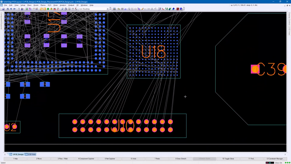
Quickly capture and lay out printed circuit boards, then verify and update designs between schematic and layout.
-
Take advantage of automated placement planning and management, self-assisted interactive sketch routing, constraint-driven routing, high-speed network tuning, and much more.
-
Access part libraries and repositories, with easy connection to component databases for quick part searches and model downloads.
-
Easily create and export design intent for PCB from MCAD environment
-
Transmit data efficiently bi-directionally between domains using the IDX data format – transfer only the data needed to propose changes
-
Use realistic 3D views of PCB components to aid design development
-
Locate PWB Components Easily Using a PWB Pathfinder
-
View component properties with a single click – no more searching for a part in a graphical environment
-
Import copper data, in the form of drafts, from the electrical domain
While Solid Edge PCB collaboration works seamlessly with Solid Edge PCB design, it can also be deployed with other industry-leading PCB design software applications that use the IDX format for ECAD-MCAD collaboration.
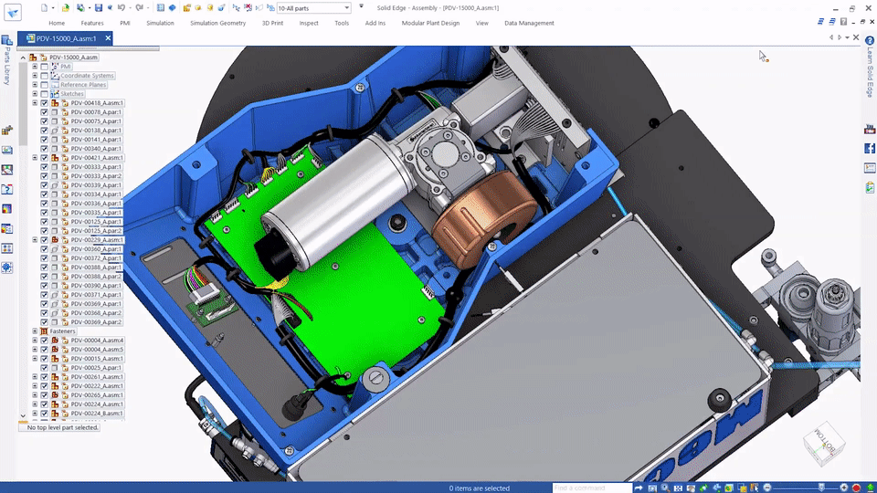
Fully integrated 3D layout with placement, constraints, design rules checking (DRC) and photorealistic visualization minimize MCAD iterations. Solid Edge PCB collaboration efficiently transmits bidirectional data between the ECAD and MCAD environments, allowing design aspects of the MCAD environment to flow into the PCB design for initial placement.
A photorealistic view of PCB components aids in accurate electromechanical product design. Solid Edge PCB Collaboration allows users to browse and import exact models, providing a true 3D view of the design that can be rotated and visually inspected for interference between ECAD and MCAD design aspects. The software supports replacing components represented in 2.5D with standard/supported 3D models available in the included library. If the 3D model is missing, the default 2.5D representation is created for that component.
Solid Edge PCB Collaboration includes a pathfinder that classifies PCB components based on their type (eg, cutouts, holdouts, coated or uncoated mounting holes, etc.) to assist users while working on an assembly. Users can quickly view properties with a single click, rather than searching for the part in the graphical environment.
Copper, an important component in PCB design, makes electrical connections between the PCB and other parts of the device possible. Knowing a project's copper layout information aids in better mechanical design and representation. Solid Edge PCB Collaboration allows the import of copper data, in the form of sketches, from the electrical domain.
Solid Edge PCB Design software tools automate PCB design in a way that even those new to PCB design can now successfully design the electronic components needed for their products.